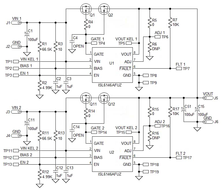
The ISL6146 represents a family of OR-ing MOSFET controllers capable of OR-ing voltages from 1V to 18V. Together with suitably sized N-channel power MOSFETs, the ISL6146 increases power distribution efficiency when replacing a power OR-ing diode in high current applications. It provides gate drive voltage for the MOSFET(s) with a fully integrated charge pump.
Demonstration Circuit 1676A showcases the LTC®4359 ideal diode controller with reverse input protection. The board includes two independent LTC4359 ideal diode circuits, sharing a common ground and operating over a 4.5V to 60V range. Each circuit comprises a load switch and ideal diode connected in series. Power to the load may be turned on and off by using the SHDN input, and the load is protect…
Demonstration circuit 1926A features the LTC4353, a dual low voltage ideal diode controller, in a typical 12A application. The LTC4353 creates two near-ideal diodes using external N-channel MOSFETs thereby replacing high power Schottky diodes and their associated heat sinks. Ideal diodes enable low loss power ORing and supply holdup applications.
Demonstration Circuit 1203 showcases two LTC4357s in a 48V, 5A application. The circuits are operational over a range of 9V to 75V and are fully independent, with the exception of a common ground.
Demonstration circuit 1899A controls two independent power rail circuits each with Hot Swap™ and ideal diode functionality provided by the LTC4228-1/LTC4228-2 dual ideal diode and Hot Swap controller.
The ISL6146 represents a family of OR-ing MOSFET controllers capable of OR-ing voltages from 1V to 18V. Together with suitably sized N-channel power MOSFETs, the ISL6146 increases power distribution efficiency when replacing a power OR-ing diode in high current applications. It provides gate drive voltage for the MOSFET(s) with a fully integrated charge pump.
The three ISL6146 evaluation boards are used to demonstrate four application configurations. All the boards have ADJ shorted to VOUT with the PCB layout having the component footprints to insert a resistor of choice between ADJ and GND to adjust the HS COMP Vth. Likewise, the VIN is connected to BIAS but these can be separated to provide an adequate BIAS voltage when OR-ing <3V supplies or if …

Thank you!
Keep an eye on your inbox for news and updates from DigiKey!
Please enter an email address
Please accept the checkbox